Article
Nanoindentation testing: How it works and where it's used
Materials science is constantly evolving, demanding increasingly precise methods to characterise mechanical properties at ever-smaller scales. Traditional hardness tests work well for bulk materials but struggle to provide accurate measurements for thin films, microscale components, and nanostructures. As technology advances, industries require techniques that can evaluate materials at the micro and nanoscale with exceptional accuracy and minimal sample damage.
To meet these demands, researchers and engineers use nanoindentation, a technique that provides a reliable way to measure properties such as hardness, elasticity, and time-dependent deformation. By applying a precisely controlled force to a material and analysing its response, they can gain valuable insights into mechanical behaviour. This level of precision is essential for improving the performance and durability of materials used in coatings, biomaterials, semiconductors, and structural components. With its versatility and high resolution, nanoindentation has become a standard method for material characterisation in both research and industry.
How Nanoindentation Testing Works
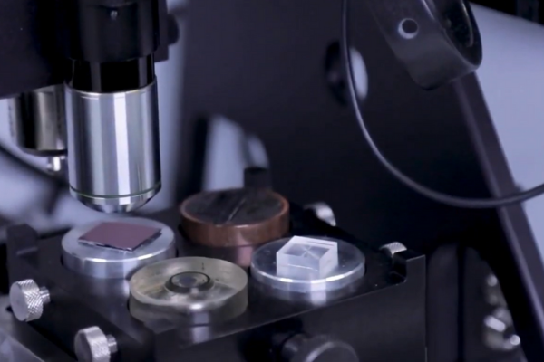
Nanoindentation involves pressing a sharp, precisely calibrated indenter into a material’s surface while continuously measuring the force applied and the resulting displacement. This data is then analysed to extract key mechanical attributes such as hardness, elastic modulus, and creep behaviour.
The Nanoindentation Process
- Preparing the Sample – Achieving accurate results requires a smooth, clean surface. If a material is too rough, it may need to be polished before testing.
- Aligning the Indenter – A high-precision microscope positions the indenter over the test location.
- Applying Force – The indenter presses into the material under controlled force while recording force-depth data in real time.
- Holding the Load (Optional) – Some tests maintain a constant force to analyse creep behaviour, which shows how the material deforms over time.
- Withdrawing the Indenter – As the indenter is removed, the material’s recovery is measured. This is to distinguish between elastic and plastic deformation.
- Analysing the Data – Using models like the Oliver-Pharr method, mechanical properties such as hardness and elastic modulus are extracted from the force-depth curve.
Types of Indenters Used
- Berkovich (three-sided pyramid): The most commonly used nanoindenter due to its well-defined geometry, making it ideal for measuring hardness and modulus in a wide range of materials.
- Vickers (four-sided pyramid): Less commonly used in nanoindentation but effective for comparing hardness values with traditional microhardness tests.
- Flat-ended cones: Used to measure the elasticity and damping of polymers as a function of time and temperature; also applied to measure the stress-strain curves of metals.
- Spherical: Utilised to test microscopic structures such as sensors or MEMS
- Cube-corner: Sharp angles make it ideal for testing fracture toughness.
Where Is Nanoindentation Used?
1. Thin Films and Coatings
The hardness, adhesion, and wear resistance of protective coatings are critical for applications in cutting tools and electronic devices. Since these films are often only a few nanometers thick, traditional testing methods are not suitable. Nanoindentation provides an effective way to evaluate these properties without damaging the underlying material.
2. Metals and Alloys
High-strength alloys used in aerospace, automotive, and structural applications must meet strict performance standards. Engineers can use nanoindentation to measure properties such as elasticity, yield strength, and hardness at the microscale. This helps refine material selection and processing techniques.
3. Polymers and Composites
Understanding the viscoelastic behaviour and long-term durability of polymers and composite materials is crucial for their use in biomedical and aerospace applications. Nanoindentation provides insights into time-dependent deformation and mechanical strength.
4. Semiconductors and Microelectronics
The structural integrity of silicon wafers, thin films, and microelectromechanical systems (MEMS) plays a key role in the reliability of modern electronics. Applying nanoindentation can help assess how these materials respond to mechanical stress and thermal expansion.
5. Biomaterials and Medical Devices
From orthopaedic implants to cartilage research, biomaterials must meet strict mechanical performance standards. Scientists use nanoindentation to study the mechanical strength of tissues and implants, leading to more durable and biocompatible solutions.
6. Ceramics and Glass
Glass and ceramic materials used in optical lenses and advanced engineering applications require high hardness and fracture resistance. Precision testing ensures these materials meet industry demands.
7. Energy Storage and Environmental Science
As the demand for advanced energy storage solutions grows, nanoindentation plays an essential part in evaluating the mechanical stability of battery electrodes, fuel cells, and solar panels.
The Advantages of Nanoindentation
Nanoindentation testing provides several benefits over traditional mechanical testing methods:
- High precision and repeatability – Suitable for extremely small material volumes.
- Minimal sample damage – Unlike bulk mechanical tests, nanoindentation leaves only microscopic indentations.
- Versatile material compatibility – Works on metals, polymers, ceramics, biomaterials, and more.
- Multi-property evaluation – Hardness, modulus, creep behaviour, and viscoelastic properties can be measured in a single test.
- Automation and high-throughput capabilities – Modern nanoindenters can perform hundreds of tests in a single session.
KLA Nanoindenters: Tools for Targeted Nanoindentation Testing
To meet the growing demand for precision at the micro and nanoscale, CN Technical Services supplies a portfolio of the KLA nanoindenters designed to support a wide range of nanoindentation applications, including thin-film characterisation, time-dependent deformation analysis, and high-throughput mechanical mapping.
Developed for in-situ testing within SEMs and other imaging systems, the NanoFlip is ideal for correlating structural and mechanical properties in microelectronics and MEMS. Its flip mechanism allows rapid switching between imaging and indentation, while NanoBlitz and CSM capabilities enable detailed modulus mapping and depth-dependent property analysis.
Optimised for soft materials and thin films, the iNano offers the sensitivity needed for nanoscale measurements. The system enables both standard hardness and modulus testing using the Oliver-Pharr method, as well as advanced viscoelastic analysis with ProbeDMA™, making it particularly effective for biomedical surfaces and compliant substrates.
This versatile system supports testing across a broad force range, ensuring its suitability for metals, ceramics, and composites. With options like NanoBlitz for rapid property mapping and high-temperature testing, the iMicro is well suited to structural materials, coatings, and demanding research environments.
A robust choice for consistent, high-throughput mechanical testing across varied material types. The G200x is commonly used for characterising ceramics, evaluating fracture toughness, and performing comprehensive mapping in semiconductor, energy, and medical applications.
Together, these systems offer complementary capabilities that align with the evolving needs of materials research. Whether the focus is on thin films, soft biomaterials, or structural micro components, the KLA nanoindenters supplied by CN Technical Services deliver the precision, repeatability, and versatility essential for reliable nanomechanical testing.
Advancing Materials Science with Nanoindentation
Nanoindentation has become a cornerstone of materials testing, providing unmatched accuracy for researchers and engineers working with thin films, microstructures, and novel materials. The ability to measure mechanical properties at the nanoscale is crucial for progressing technology in industries such as aerospace, electronics, healthcare, and energy storage.
For laboratories and manufacturers that require precise material characterisation, CN Technical Services provides a selection of advanced nanoindenters designed for both research and industrial applications. Our expertise in high-resolution mechanical testing helps support innovation in materials development. This ensures industries can continue to push the boundaries of performance and reliability. Uncover more information about our range of nanoindentation equipment here.