Article
Synchronising SEM and nanomechanical data with in-situ nanoindentation
Materials behave in complex ways at the nanoscale. A thin film that appears uniform might harbour hidden fractures, while a composite material could fail at specific boundaries despite its bulk properties indicating strength. To engineer more reliable materials, it's essential to understand both structure and mechanical behaviour simultaneously, in real time.
This integration is achieved through in-situ nanoindentation, where nanoindentation is performed directly inside a Scanning Electron Microscope (SEM) chamber. SEM provides high-resolution images of material surfaces. It reveals fine structural details such as grain boundaries, cracks, and coating interfaces. Meanwhile, nanomechanical testing, particularly nanoindentation, quantifies mechanical properties like hardness, elasticity, and adhesion at the nanoscale.
Synchronising these techniques through in-situ nanoindentation allows researchers to observe and measure material behaviour in real time. They're able to produce a more complete picture of how microstructure influences mechanical performance. In-situ nanoindentation therefore bridges the gap between imaging and mechanical data, enabling more accurate failure analysis and better material optimisation.
Why Synchronisation Matters: Connecting Structure to Performance
Materials do not fail randomly; weaknesses often develop at microstructural features like grain boundaries or defects. Understanding these failure mechanisms requires capturing both the structural and mechanical response of a material simultaneously.
For example, a semiconductor thin film may appear smooth under SEM. However, nanoindentation might reveal unexpectedly low hardness in certain regions. Without synchronised imaging, it’s difficult to determine whether this weakness is due to material composition, microvoids, or structural inconsistencies. When SEM and nanomechanical data are combined, every mechanical data point is linked to a specific structural feature, turning raw numbers into meaningful insights.
This approach enhances material characterisation in several ways. Determining whether cracks initiate at grain boundaries, phase transitions, or defects enables more precise failure analysis. Targeted mechanical testing ensures that indentation focuses on regions of interest, such as coatings, interfaces, or specific microstructural features. Additionally, linking microstructure to mechanical properties allows for better material optimisation, improving performance and durability.
In-Situ Nanoindentation: The Key to Synchronisation
Traditional nanoindentation is performed ex-situ, meaning it takes place outside the SEM. While this provides mechanical data, it lacks direct visualisation of deformation events. In-situ nanoindentation, however, integrates the nanoindenter directly into the SEM chamber. It can therefore capture both force-displacement data and real-time imaging of material response.
Adopting in-situ nanoindentation not only enables researchers to see how materials deform but also ensures that mechanical property measurements are precisely aligned with structural features. As force is applied, the nanoindenter records load-depth curves, hardness values, and elastic modulus, while the SEM captures the corresponding physical changes in the material. The simultaneous collection of nanomechanical and imaging data provides a deeper understanding of how microstructural characteristics, such as grain size, phase boundaries, and dislocation movements, affect mechanical behaviour.
Establishing a direct correlation between structural changes and mechanical response gives researchers a more complete analysis of material performance. This integration is particularly useful for studying coatings, thin films, and other nanoscale structures where small variations in composition or defects can significantly impact overall mechanical stability.
Advantages Over Traditional Methods
Synchronising SEM with nanomechanical testing offers several advantages over traditional ex-situ methods:
- Direct Visualisation of Deformation: In-situ testing eliminates the need to infer material behaviour from force-displacement curves alone. Researchers can see cracks forming, dislocations moving, and phase transitions occurring in real time.
- Elimination of Alignment Errors: In ex-situ testing, repositioning the sample between SEM and nanoindentation systems could cause misalignment. Conducting tests in-situ ensures perfect spatial correlation between mechanical measurements and SEM imaging.
- More Accurate Failure Analysis: Examining mechanical behaviour alongside SEM images provides a precise understanding of failure mechanisms, helping improve material durability and performance.
Applications: Where Synchronisation Makes an Impact
The ability to simultaneously see and measure how materials respond to stress has wide-reaching implications across various industries:
Semiconductor Manufacturing
Thin films and coatings in microelectronics must withstand mechanical stress without failure. Synchronising SEM and nanomechanical data ensures these layers maintain both structural integrity and functional reliability, reducing the risk of premature failure in semiconductor devices.
Biomedical Implants & Biomaterials
Implant materials need to mimic the mechanical behaviour of biological tissues while maintaining long-term stability. Combining SEM imaging with nanomechanical testing allows researchers to fine-tune elasticity, adhesion, and wear resistance, leading to improved implant performance and longevity.
Metallurgy & Advanced Materials
From high-strength alloys to nanostructured materials, in-situ nanoindentation helps scientists understand how grain boundaries, phase transitions, and microstructural variations influence mechanical performance. This paves the way for stronger, more resilient materials.
Bridging Structure and Performance with In-Situ Nanoindentation
Understanding how materials respond to stress requires more than just imaging or mechanical testing alone. Synchronising SEM and nanomechanical data with in-situ nanoindentation enables researchers to see and measure material behaviour in real time, making it possible to connect structural features directly to mechanical performance. This approach leads to better failure analysis, improved material design, and more reliable performance in critical applications.
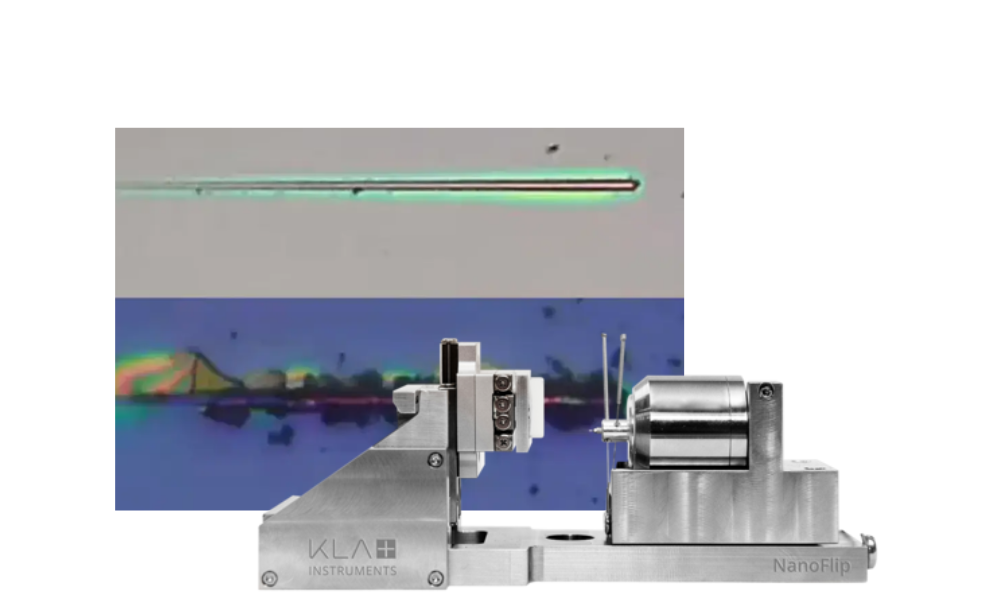
For those looking to utilise this capability, the NanoFlip® Nano Indenter from CN Technical Services offers a powerful solution. Designed for integration within SEM chambers, it enables high-precision nanomechanical testing while maintaining alignment with real-time imaging. With tools like the NanoFlip®, researchers can push material science further, developing more robust, resilient, and efficient materials for the future.