Article
How to Overcome Nanomechanical Testing Pain-Points in Materials R&D
Nanomechanical testing has become integral to materials research and development (R&D), helping to investigate the mechanical behaviour of materials at the nanoscale. Mechanical behaviour testing methods like nanoindentation and micro-pillar compression have supported researchers in measuring key material properties like hardness, modulus, and yield strength with pinpoint precision. However, despite their capabilities, techniques such as these come with a set of recurring challenges that can make it harder to obtain accurate and reliable results.
The Role of Nanomechanical Testing in Materials Research
At its core, materials R&D focuses on developing materials that meet strict performance criteria in complex environments, spanning applications like jet engines and microchips. As these materials become more sophisticated and smaller in scale, traditional testing methods often fall short. For instance, techniques like bulk tensile testing and macro-scale hardness measurements tend to lack the resolution to capture localised behaviour in increasingly small and complex materials.
Characterising mechanical responses at the nanoscale requires techniques with far greater resolution, such as nanomechanical testing. Tools designed for nanomechanical testing, including nanoindentation, help uncover mechanical behaviour at fine structural scales. These behavioural insights are vital for improving performance, durability, and reliability in everything from coatings to composites. By capturing accurate, repeatable data and linking it to real-time structural changes, researchers can better understand what’s happening below the surface of a material.
Understanding the Pain-Points in Nanomechanical Testing
Despite the importance of nanomechanical testing in materials R&D, researchers still face persistent challenges that can impact data quality and interpretation.
Challenging Sample Preparation
Sample preparation remains one of the most technically demanding aspects of nanomechanical testing. Whether the focus is on thin films, layered materials, or micro-pillars, preparing samples with micron-level accuracy can be challenging. Techniques such as Focused Ion Beam (FIB) milling are widely used, but they can introduce defects or distortions that can impact the accuracy of test results. Even minor issues, like slight misalignment or surface damage, can throw off measurements. This is especially problematic when working with materials that are sensitive to processing or have complex structures.
Mitigation strategies:
-
Apply low-current FIB settings to reduce ion beam damage
-
Design samples for direct transfer between prep and SEM stages
-
Align samples using fiducial markers or integrated positioning stages
Thermal Drift and Environmental Instability
Measurements in nanomechanical testing can be significantly affected by environmental conditions. Thermal drift, caused due to small fluctuations in temperature, can alter indenter position over time, while mechanical vibrations or airflow disturbances can introduce unwanted noise. These challenges are particularly troublesome in long-duration or elevated-temperature tests, where maintaining a stable testing environment is crucial.
Mitigation strategies:
-
Utilise thermal enclosures or localised temperature control
-
Incorporate active drift correction algorithms
-
Employ vibration isolation tables or damping systems
-
Monitor ambient conditions and limit airflow around the test area
Size Effects and Contact Area Uncertainty
Material properties at small scales often vary with indentation depth, a phenomenon known as the size effect, where hardness tends to increase as the indentation becomes shallower. This makes it difficult to compare results across tests, which can lead to inaccurate interpretations if the size effect is not properly accounted for. Accurately defining the contact area between the probe and sample adds further complexity, particularly for soft, composite, or uneven surfaces. Without measurement and correction, such factors can distort results and reduce data reliability.
Mitigation strategies:
-
Use continuous stiffness measurement (CSM) to track stiffness in real time
-
Calibrate probes carefully and account for surface roughness
-
Apply modelling to estimate the contact area for irregular geometries
-
Combine mechanical testing with imaging to refine contact interpretation
Lack of In Situ or Operando Observation
In many nanomechanical testing setups, material deformation occurs beyond view, forcing researchers to rely on indirect data to interpret what took place. Important mechanisms, such as crack propagation or dislocation movement, can be overlooked, limiting the accuracy of mechanical analysis.
Mitigation strategies:
-
Integrate mechanical testing stages into scanning or transmission electron microscope (SEM/TEM) systems to observe deformation as it occurs
-
Employ digital image correlation (DIC) or electron backscatter diffraction (EBSD) for structural mapping
-
Capture sequential images to track progressive material changes
-
Utilise real-time imaging to correlate force-displacement data with deformation
Complex Data Interpretation and Disconnected Measurements
Nanomechanical testing generates a wealth of data, from mechanical curves to structural images, all of which need to be aligned to extract meaningful insight. When these data streams remain isolated or are processed manually, interpretation becomes slow and prone to error. The absence of integrated tools often stalls progress and limits the clarity of conclusions.
Mitigation strategies:
-
Use unified software platforms for mechanical and imaging data to streamline workflows and reduce the risk of mismatched or lost information
-
Link test data to microstructural features using image correlation, enabling clearer insights into how structural variations affect mechanical behaviour
-
Apply AI or machine learning to automate data processing
Best Practices for Materials R&D Teams
Material R&D teams should consider the following practices to tackle the challenges of nanomechanical testing:
-
Utilise sample preparation methods that minimise damage and preserve structural integrity
-
Control environmental conditions rigorously to reduce drift and variability
-
Employ techniques like CSM to handle size effects and improve property accuracy
-
Implement integrated software tools to correlate mechanical and structural data
-
Work with multiscale models to translate nanoscale findings into engineering solutions
By refining how nanomechanical testing is performed and interpreted, materials R&D teams can uncover deeper insights and facilitate innovation.
Helping Materials R&D Teams Overcome Nanomechanical Testing Pain-Points
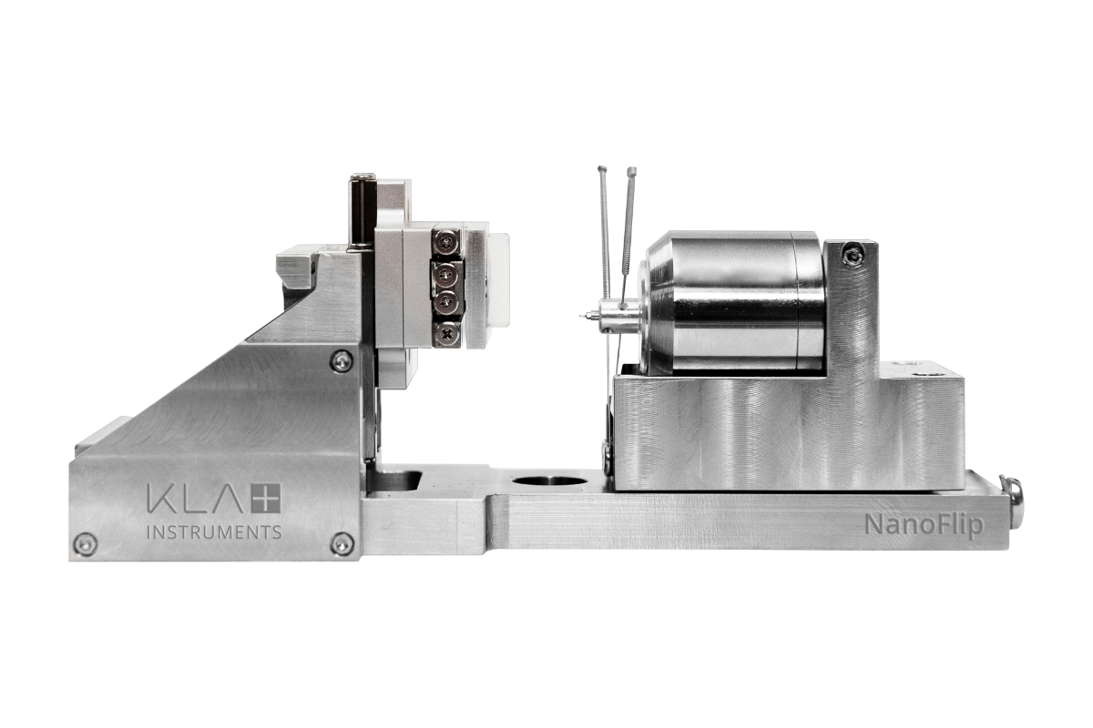
Solving persistent nanomechanical testing challenges begins with the right tools. CN Tech provides targeted solutions for materials R&D, including the NanoFlip for in-situ SEM nanoindentation, nanoscratch platforms for thin film assessment, tribometers for wear analysis, and CMP tools for polishing studies. These technologies are built to deliver accurate results, streamline complex workflows, and support deeper material insights. Reach out to us today for more information about our available products for nanomechanical testing.