ResiScope III
ResiScope™ III is a cutting-edge module for Atomic Force Microscopy (AFM) that enables high-precision electrical measurements offering capabilities that extend beyond traditional Scanning Spreading Resistance Microscopy (SSRM) in measuring resistance and current over an exceptionally wide range, making it an indispensable tool for nanoscale electrical characterisation.
Key Features
- Superior accuracy and reduced background noise (Noise floor: < 30 fA RMS)
- Simultaneous PFM + ResiScope measurements
- Full integration with NanoSolution software
- Access to all new future features and updates
- Enhanced compatibility with advanced AFM modes
- Resistance Range: 10² to 10¹² Ω
- Current Range: 50 fA to 1 mA
- Advanced auto-ranging capabilities
- Real-time current protection system
Manufacturer
CSI
CSInstruments is a French scientific equipment manufacturer specialised in the conception of Atomic Force Microscope and options designed for existing AFM (Nano-Observer AFM, Resiscope™, High Voltage Amplifier, Magnetic modules). The product range proposed by CSInstruments is designed and manufactured to help the scientific community to achieve nanometre performances that meet the research needs and requirements for actual and future nanoscience applications.
CSInstruments was founded by a team of experts working in AFM field for more than 20 years, starting as pioneer with some historical manufacturers. CSInstruments activity is also based on a qualified and dynamic team, experienced in the fields of mechanics, electronics and data processing. This expertise ensures innovation and performance in the production of AFM and achieves an excellent price/performance ratio!
How does Resiscope III work?
ResiScope™ III is an advanced module for Atomic Force Microscopy (AFM) that enables high-precision electrical measurements at the nanoscale. Here's an overview of its working principle:
-
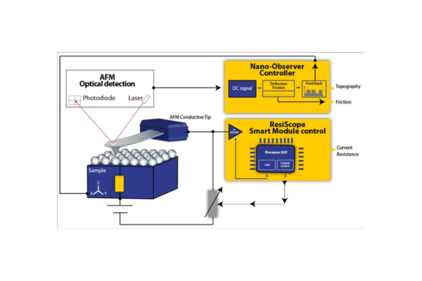
Conductive Probe:
A conductive AFM tip is used to scan the sample surface.
The tip acts as one electrode, while the sample acts as the other. -
Voltage Application:
A DC bias voltage is applied between the tip and the sample. -
Current Measurement:
As the tip scans across the surface, it measures the current flowing between the tip and the sample. The current range can be from 100 fA to 1 mA. -
Resistance Calculation:
Using the applied voltage and measured current, the system calculates the local resistance. The resistance range covered is from 10² to 10¹² ohms. -
Fast Auto-Ranging:
A fast processor-driven auto-ranging system allows for real-time adjustment of the measurement range. This enables accurate measurements across a wide range of conductivities without manual intervention. -
Current Limit-Protective Resistance:
Current limitation helps to minimize undesired current-related effects like local oxidation or bimetallic effect. -
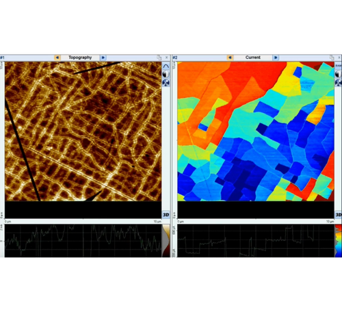
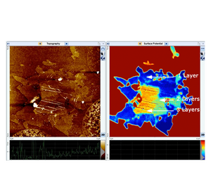
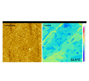
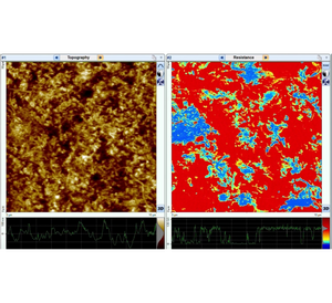
Simultaneous Resistance/Current/Topography:
While measuring the topography, the system simultaneously captures resistance and current data. This enables comprehensive correlation between physical and electrical properties. -
Compatible with All AFM Modes:
ResiScope III is compatible with all AFM modes such as EFM/MFM and standard KFM. Notably compatible with: PFM/ResiScope simultaneously to define real piezo/ferroelectric domains. Contact mode, oscillating modes, and Soft-IC mode for quantitative electrical measurements on soft samples -
Data Processing and Visualization:
The collected data is processed in real-time to create high-resolution maps of current and resistance. These maps can be overlaid with topography data for integrated analysis. -
Environmental Control:
Measurements can be performed in air, controlled atmospheres, and with temperature control.
Advanced capabilities demonstrated in applications like VO₂ under temperature variation.
The unique design of ResiScope III allows for unprecedented sensitivity and range in electrical measurements, making it a powerful tool for nanoscale electrical characterization across a wide range of materials and applications.
Specifications
| Resistance Measurement Range | 10² to 10¹² ΩCurrent |
| Measurement Range | 100 fA to 1 mA |
| Voltage Range | ±10 V (adjustable) |
| Measurement Speed | Up to 10 kHz (100 μs per measurement) |
| Auto-Ranging | Real-time, processor-driven |
| Current Control | Active, real-time adjustment |
| Noise Level | < 10 fA RMS |
| Compatible AFM Modes | Contact Mode Oscillating Mode Force Spectroscopy |
| Integration Capabilities | HD-KFM MFM/EFM PFM Environmental Compatibility:Air Controlled Atmospheres Liquids |
| Topography Acquisition | Simultaneous with electrical measurements |
| Data Output | Real-time resistance and current mapping |
| Spatial Resolution | Dependent on AFM tip radius (typically < 10 nm) |
| Software | Integrated with Nano-Observer II control software |
| Data Analysis | Built-in analysis tools for electrical property mapping |
| Compatible Probes | Wide range of commercially available conductive AFM probes |
| Scan area | Up to 100 μm x 100 μm |
| Operating Temperature | 10°C to 40°C (standard), extended range available |
| Humidity Range | < 80% RH, non-condensing |

Industries
- Materials Science
- Life Sciences
- Semiconductors and Electronics
- Academics
- Others (includes solar cells, geoscience, forensic science, and food technology)
Applications
Semiconductor Analysis
Doping profiling, defect analysis, 2D semiconductors, junction studies
Nanoelectronics Research
Nanowires, nanotubes, graphene, quantum dots, molecular electronics
Material Science
Conductive materials, composites, corrosion studies, novel materials
Polymer and Composite Studies
Conductive polymers, blends, carbon nanotube composites, organic electronics
Thin Film Characterisation
Uniformity analysis, dielectric films, TCO films, solar cell materials
Energy Materials
Battery electrodes, fuel cells, photovoltaics, thermo electrics
Biomaterials and Bioelectronics
Conductive biomaterials, neural interfaces, biosensors
Advanced Coatings
Anti-static coatings, conductive coatings, smart coatings
Memory and Data Storage
RRAM, magnetic media, phase-change memory, spintronics
Optoelectronics
Photodetectors, LEDs, OLEDs, photovoltaic junctions
Related Products
Service Support
Comprehensive repairs and servicing
Annual Support Programs
Your metrology instrumentation is a major investment that is critical to your business operation and success. In today’s competitive climate, it is more important than ever to extend the functionality and peak performance of your metrology equipment years beyond the expiration of your factory warranty. CN Tech’s Support Programs will help ensure that your investment is protected, and that you and your instrument’s are always operating at peak performance.
With over 20 years’ experience servicing and repairing you can be assured that your system is in safe hands. The independent services we offer include system relocation, maintenance visits, parts and consumables, and break down interventions.
CN Tech’s Support Programs are an economical way to guarantee optimal working condition:
- Annual Preventive Maintenance
- Priority Technical Assistance
- Preferred Parts Availability
- On-Site User Training
- Remote Diagnostics
- No surprise repair expense and much more!
Support Contact Example
An example of our service and support contracts are shown below:
Metrology & Instrumentation Annual Support Programs 2024/25
CN Tech's Support Programs will help ensure that your investment is protected, and that you and your instrument’s are always operating at peak performance.