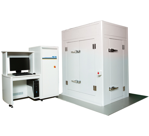
PHI 710
Multi-Technique Scanning Auger Nanoprobe
Key Features
- High spatial resolution Auger and secondary electron (SE) imaging
- Superior Auger imaging of real world (rough) surfaces
- Cylindrical Mirror Analyser (CMA) with high energy resolution capability
- Robust insulator analysis capability
- Multi-technique solutions for in-situ characterisation
Manufacturer
Physical Electronics
Physical Electronics (PHI) is a subsidiary of ULVAC-PHI, the world's leading supplier of UHV surface analysis instrumentation used for research and development of advanced materials in a number of high technology fields including: nanotechnology, microelectronics, storage media, bio-medical, and basic materials such as metals, polymers, and coatings.
Capabilities
- Microstructure Analysis on Real World Samples
- Nanoscale Thin Film Analysis
- Superior Auger Imaging
Exceptional Spatial Resolution
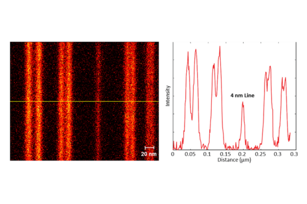
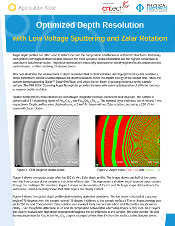
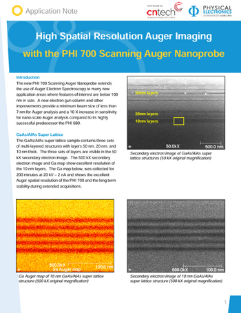
High performance electron optics, precision sample handling, and advanced vibration and thermal isolation provide a superior environment for anno-scale Auger imaging and analysis at working magnifications of 500,000 X and higher. A robust imaging registration capability ensures long term image stability when it is needed. The sample to the right presents the cross-section of alternating layer of GaAIAs and GaAs of known thickness in a spatial resolution reference sample. On the left is an AI Auger map and to the right is an AI line scan that was extracted from the map data. The shape of the single 4nm line acquired for the 24 hours demonstrates the high stability of the 710 and the effectiveness of its image registration software.
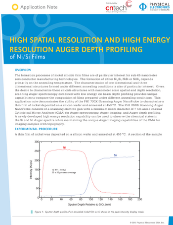
Nanoscale Thin Film Analysis
The PHI 710's floating column ion gun provides a broad range of depth profiling capabilities. At higher ion beam energies (2-5 keV) structures several microns thick can be routinely depth profiled. For thin and ultra-thin films (>5 nm) the floating ion column can be used to efficiently sputter with ion bean energies of 100 - 500 eV. The use of lower accelerating voltages reduces sputter mixing that could broaden the observed interfaces in an ultra-thin film structure.
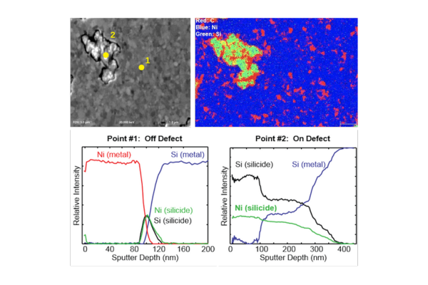
The sample shown in the SE image to the left contains a defect that appeared in a thin nickel film deposited on silicon substrate after it was annealed to form a nickel silicide at the interface. A 500 V multi-point argon sputter depth profile showed the expected formation of Ni silicide at the interface at point 1. However, at point 2 a complex multiphase silicide is observed at the defect. The chemical state information was obtained using linear least squares fitting to process the high energy resolution spectra that were collected.
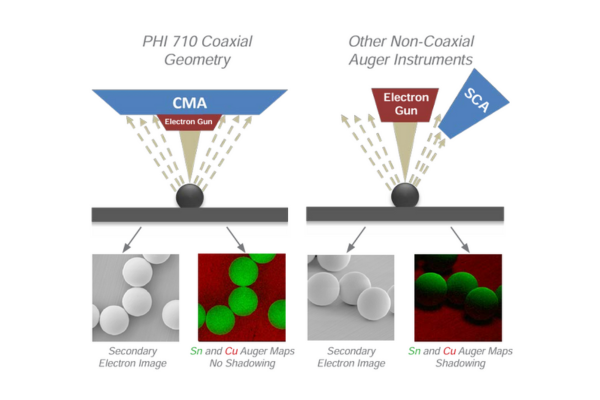
Unobstructed Visualisation
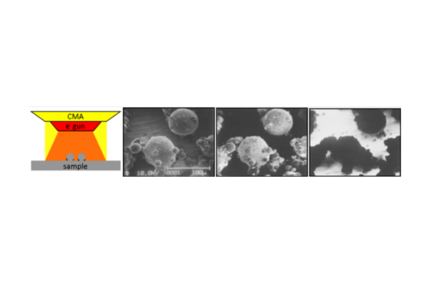
PHI's coaxial electron gun and analyser geometry provides the sensitivity and unobstructed vision needed to fully characterise the microstructures that exist on most real-world samples. Instruments with non-coaxial geometry suffer from geometric effects that dramatically reduce instrumental sensitivity and create shadows that limit the usefulness of compositional images. With the 710's coaxial geometry, Auger data is obtained from all sides of particulates and between particles with equally high sensitivity providing Auger maps with meaningful compositional information.
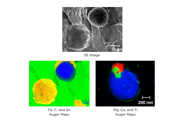
Excellent Imaging on Real-World Materials
The coaxial analyser and electron gun geometry provided by the PHI 710 produces a complete compositional picture of the area selected for analysis. The analyser will provide data from every location the electron gun probed. Black areas in maps are usually not caused by sample roughness and analyser shadowing, but instead indicate the presence of another element. The secondary electron image (top) shows the microstructure of a ductile iron fracture surface including graphite nodules and craters where graphite nodules have fallen our because of the fracture. The AES maps (left) show the ability to map across the graphite nodule and the crater where Sn has segregated to the nodule / iron interface. AES maps (right) show the complex composition of a small precipitate. Only PHI Auger instruments with coaxial electron gun and analyser geometry provide such a complete compositional picture of a rough sample surface.
Specialised Solutions for In-Situ Characterisation
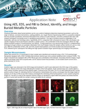
The PHI 710 has multiple optional technique add-ons and accessories for specialised experiments. Liquid metal focused ion bean (FIB) allows for in-situ cross-sectioning of particles, defects and coatings. Energy dispersive X-ray Spectroscopy (EDS) detector provides qualitative and quantitative elemental information. The windowless software driven motor-controlled detector has a short working distance for wide acceptance angles. Backscattered Electron Detector (BSE) provides topographic information and compositional information of the sample by using a four-quadrant detector. Electron Backscatter Diffraction (EBSD) detector provides information about crystal structure and grain orientation.
The secondary electron image (top left) shows a particle within a titanium zirconium passivated aluminium sample. The particle was first observed by SEM/EDS and the EDS map (top right) of the region showed that the particle contained iron. A FIB cut across the centre of the particle (SEM image, bottom left) reveals the iron containing particle is platelet shaped and buried beneath the sample surface (bottom right). Analysis of these types of buried features requires the complementary analytical capabilities of EDS, FIB, and AES.
Solutions for Insulating Materials
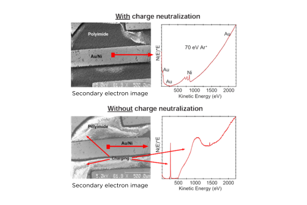
The PHI 710's floating column ion gun can be effectively used at very low energies to facilitate the analysis of many electrically insulating samples. This method is particularly effective on inorganic materials such as ceramics and electronics packages.
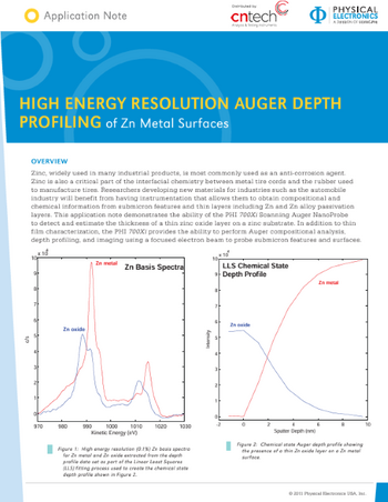
High Energy Resolution
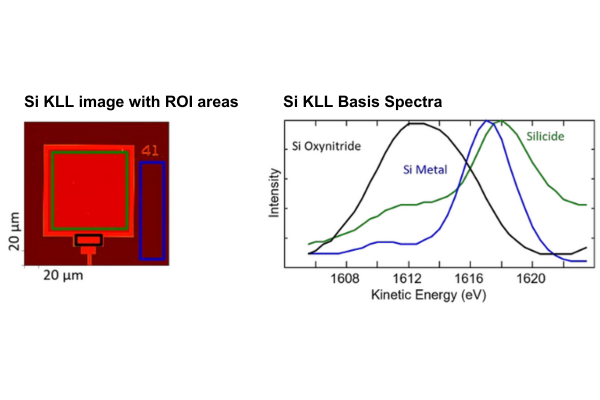
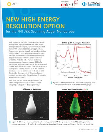
The 710's high energy resolution mode of operation provides for continuous adjustment of the analyser energy resolution to as low as 0.1%. The high energy resolution capability can be used to enhance the chemical information content of spectra and AES images while maintaining all the advantages of the CMA with a coaxial electron source for obtaining data with high sensitivity and nearly eliminating topography induced artefacts. Additionally, the PHI 710 Scanning Auger Nanoprobe has no incorporated new electronics and data interpretation software to facilitate chemical state mapping based on images that contain a spectrum at each pixel.
The Si KLL peak area image from a semiconductor bond pad (left) is shown with three regions of interest. The extracted basis spectra from each ROI (right) reveals three distinct chemical states of silicon. This is enabled by the spectral window imaging mode, where in a Si KLL spectrum is collected and stored for each image pixel.
Nanovolume Analysis
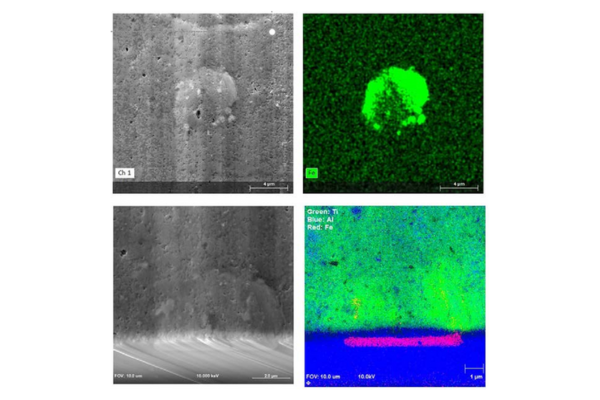
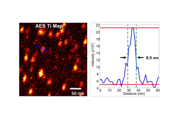
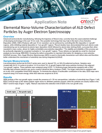
The PHI 710's high spatial resolution combined with the coaxial CMA analyser and the inherent shallow information depth of Auger Electron Spectroscopy enable nano-volume characterisation of small particles. Defect particles, which can be detrimental to semiconductor device performance, are readily imaged and elementally quantified using state of the art technology.
Defect particles present during an atomic layer deposition / atomic layer etching process are readily imaged and characterised. These particles were found to consist of an elevated titanium concentration compared to the surrounding substrate. From then titanium map (right), a <9 nm diameter nanoparticle is clearly identified, demonstrating the PHI 710's superior nano-volume analysis capability.
Software
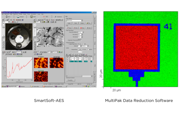
SmartSoft-AES
- Intuitive, fully integrated, Windows™ software platform controls all instrument functions
- Session tabs guide you through the analysis process
- Seamless interface to PHI MultiPak data reduction software
MultiPak Data Reduction Software
PHI MultiPak is the most comprehensive data reduction and interpretation software package available for electron spectroscopy. The tasks of spectral peak identification, quantification, extracting chemical state information, detection limit and image enhancement are addressed with an array of powerful and easy-to-use software tools for spectra, line scans, images and depth profiles.
Colour overlay of elemental silicon (green), silicide (red) and silicon oxynitride (blue) images created using the Linear Least Squares fitting algorithm in MultiPak to extract multiple silicon chemical state images from the elemental silicon image.
Downloads
PHI 710 Brochure

Using Low Energy Ions for Charge Neutralisation in PHI Scanning Auger Nanoprobes
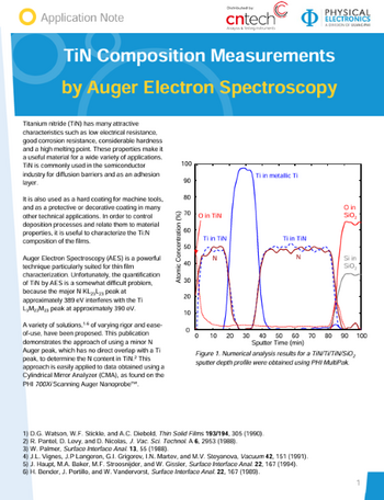
TiN Composition Measurements by Auger Electron Spectroscopy
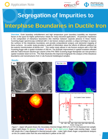
Segregation of Impurities to Interphase Boundaries in Ductile Iron
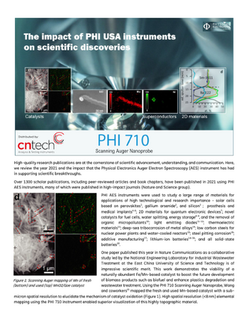
The Impact of PHI USA Instruments on Scientific Discoveries
Optimised Depth Resolution with Low Voltage Sputtering and Zalar Rotation
New High Energy Resolution Option for the PHI 700 Scanning Auger Nanoprobe
High Spatial Resolution Auger Imaging with the PHI 700 Scanning Auger Nanoprobe
High Spatial Resolution Auger Imaging of Highly Topographic Samples
High Spatial Resolution and High Energy Resolution Auger Depth Profiling of Ni/Si Films
High Energy Resolution Auger Depth Profiling of Zn Metal Surfaces

Fracture Analysis of an Embrittled Low Alloy Steel Rotor Blade from an Operating Steam Turbine
Using AES, EDS, and FIB to Detect, Identify, and Image Buried Metallic Particles
Elemental Nano-Volume Characterisation of ALD Defect Particles by Auger Electron Spectroscopy
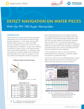
Defect Navigation on Wafer Pieces with the PHI 700 Auger Nanoprobe

Corrosion Analysis in Metallurgical Samples: A PHI 710 Multi-technique Approach
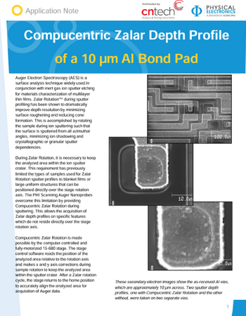
Compucentric Zalar Depth Profile of a 10 µm AI Bond Pad
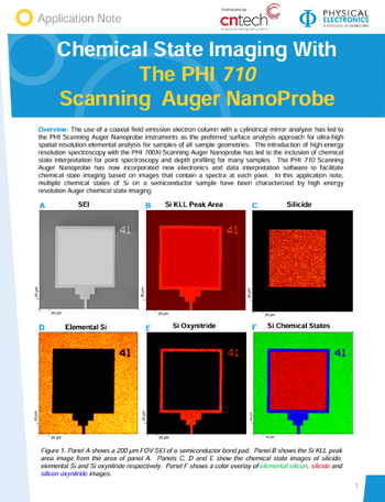
Chemical State Imaging with the PHI 710 Scanning Auger Nanoprobe
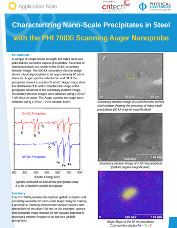
Characterising Nano-Scale Precipitates in Steel with the PHI 700Xi Scanning Auger Nanoprobe
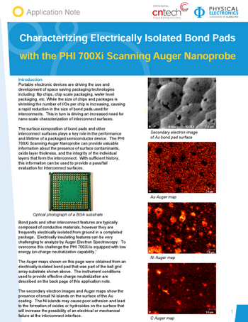
Characterising Electrically Isolated Bond Pads with the PHI 700Xi Scanning Auger Nanoprobe
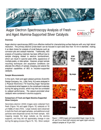
Auger Electron Spectroscopy Analysis of Fresh and Aged Alumina-Supported Silver Catalysts
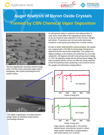
Auger Analysis of Boron Oxide Crystals Formed by CBN Chemical Vapour Deposition
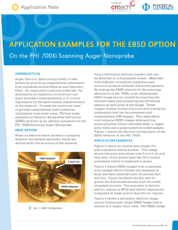
Application Examples for the EBSD Option on the PHI 700Xi Scanning Auger Nanoprobe
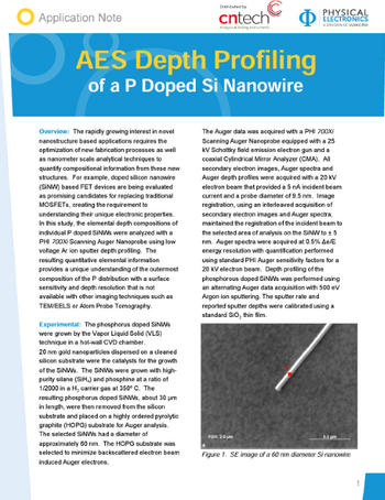
AES Depth Profiling of a P Doped Si Nanowire
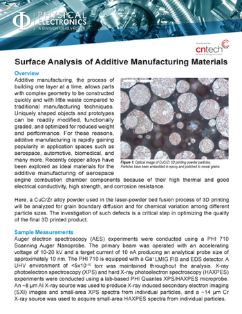
Surface Analysis of Additive Manufacturing Materials
Service Support
Comprehensive repairs and servicing
Annual Support Programs
Your metrology instrumentation is a major investment that is critical to your business operation and success. In today’s competitive climate, it is more important than ever to extend the functionality and peak performance of your metrology equipment years beyond the expiration of your factory warranty. CN Tech’s Support Programs will help ensure that your investment is protected, and that you and your instrument’s are always operating at peak performance.
With over 20 years’ experience servicing and repairing you can be assured that your system is in safe hands. The independent services we offer include system relocation, maintenance visits, parts and consumables, and break down interventions.
CN Tech’s Support Programs are an economical way to guarantee optimal working condition:
- Annual Preventive Maintenance
- Priority Technical Assistance
- Preferred Parts Availability
- On-Site User Training
- Remote Diagnostics
- No surprise repair expense and much more!
Support Contact Example
An example of our service and support contracts are shown below:

Metrology & Instrumentation Annual Support Programs 2024/25
CN Tech's Support Programs will help ensure that your investment is protected, and that you and your instrument’s are always operating at peak performance.