Article
Performing electrical measurements using atomic force microscopes
Nanoscale materials and increasingly intricate device architectures are pushing traditional electrical measurement tools, like four-point probe systems, impedance spectroscopy, and macroscale Kelvin probe techniques, beyond the spatial resolution they can reliably achieve. These approaches smooth over local fluctuations, frequently overlooking the subtle electrical variations that drive behaviour in semiconductors, energy-storage materials, and soft matter systems. Atomic Force Microscopes (AFMs), originally developed for high-resolution surface imaging, now provide a way to reliably measure electrical properties with precision.
Why Atomic Force Microscopes Are Used for Electrical Measurements
Since their introduction in the late 1980s, AFMs have evolved from imaging tools into versatile platforms for nanoscale characterisation. Unlike optical or electron microscopes, AFMs rely on a sharp probe that physically interacts with the sample surface. This allows them to measure not only topography but also mechanical, chemical, and electrical properties. For electrical measurements, the conductive tip acts as a nanoscale electrode capable of detecting current, voltage, capacitance or electromechanical response with high spatial resolution.
Because they operate in air, liquid or controlled environments, and work effectively with both conductive and insulating materials, AFMs offer unique advantages for studying systems that are too delicate, heterogeneous or spatially complex for traditional techniques. Such qualities make them especially valuable for capturing high-resolution electrical data in advanced materials research and device development.
How to Perform Electrical Measurements with an AFM
Carrying out electrical measurements with an AFM involves a series of coordinated steps, from preparing the sample and selecting the right mode to scanning the surface and interpreting the results. Each stage plays a role in ensuring that the data collected is accurate, consistent and meaningful.
Preparing for Measurement
Accurate electrical measurements with an AFM begin long before scanning starts. Success depends on mechanical stability, effective sample preparation, and the thoughtful selection of both probe and measurement mode.
Sample Handling
The sample surface should be clean, smooth and securely mounted. When working with insulating materials, a conductive path to ground is often required to prevent charge buildup or measurement artefacts.
Probe Selection
Electrical modes use conductive tips, typically coated with materials like platinum or gold. Tip selection should align with the specific measurement requirements and account for both electrical sensitivity and the mechanical characteristics of the sample. For more hard wearing samples, platinum silicide or diamond AFM probes are typically used.
Environmental Conditions
External factors such as vibration, temperature shifts and ambient noise can affect signal quality. Electrical measurements benefit from a controlled environment, including consistent humidity and minimised interference.
Selecting the Appropriate Mode
Atomic Force Microscopes support a variety of electrical modes, each suited to different materials and measurement objectives.
Conductive AFM (C-AFM)
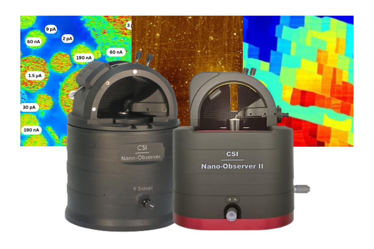
By applying a voltage between the probe and the surface, C-AFM records local current flow as the tip moves across the sample. This approach is particularly effective for identifying defects, assessing conductivity in thin films, and revealing inhomogeneities in electronic materials like semiconductors, metal oxides, 2D materials, perovskite layers, and conductive polymers. Quantitative electrical characterisation is further supported through CSI’s Resistivity mode (ResiScope™ III), which builds on C-AFM through measuring current-bias relationships under controlled tip-sample contact to generate high-resolution resistivity maps. With an extremely wide dynamic range, the CS Instruments ResiScope III measures 10² to 10¹² Ω in resistance, 50 fA to 1 mA in current.
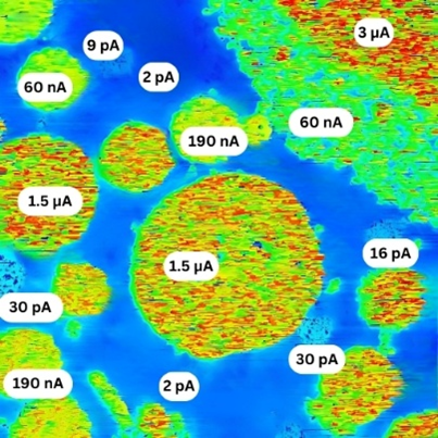
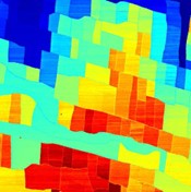
Figure 1: (Left to right) Polymer Battery Characterization, identifying high-conductivity (µA) vs. low-conductivity (pA) domains. Epitaxially growth Vanadium Oxide (VO2) with different levels of conductivity. SiC doping levels: from 100 Ω to 1 MΩ across small lateral distances
Kelvin Probe Force Microscopy (KPFM)
KPFMs, also known as Kelvin Force Microscopy (KFM), senses variations in surface potential through detecting electrostatic forces between the tip and the sample. Researchers use it to analyse work function shifts, explore doping levels and investigate trapped charge regions in electronic devices like semiconductor transistors, solar cells, resistive-switching memories, and organic thin-film components. For more advanced work, High-Definition Kelvin Force Microscopy (HD-KFM) can enhance traditional KFM by offering single-pass operation and greatly improved sensitivity and lateral resolution, as well as additional capabilities, such as dC/dZ mapping, which ensures it can resolve subtle variations in surface potential and dielectric behaviour that are critical for analysing semiconductor interfaces, heterostructures, and emerging nanoscale device architectures, like 2D-material transistors and ferroelectric memories.
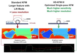
Figure 2 - Optimized single pass KFM (HD-KFM III) with higher sensitivity and resolution than standard KFM in lift mode
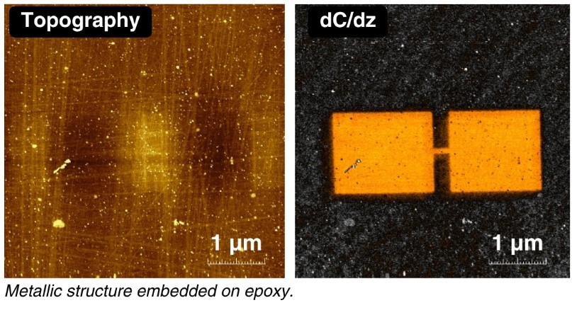
Figure 3 - Topography (Left): Provides a detailed surface morphology map, showing the overall structure of the metallic features embedded in the epoxy. HD-KFM III (Right): Reveals intricate electrical details (dC/dz) of the metallic structure embedded within the epoxy that are not visible in the topography. This advanced mode enables precise visualization of the electronic contrast, providing critical insights into the material's composition and distribution.
Electrostatic Force Microscopy (EFM)
EFM is commonly utilised to examine surface charge distribution and assess dielectric behaviour in polymers and insulating materials including oxide dielectrics, ceramic insulators, and polymer-ceramic composites where charge tapping and dielectric heterogeneity are important. The tip is lifted above the surface to detect long-range electrostatic interactions during scanning.
Scanning Microwave Impedance Microscopy (SMIM)
SCM uses a high-frequency signal to monitor changes in capacitance as the tip scans over the surface. It provides detailed insight into dopant concentration and subsurface structures, making it useful for characterising semiconductor cross-sections.

Figure 4 - Sample of static random-access memory (sRAM) using Scanning Microwave Impedance Microscopy (sMIM) mode (13mm scan area) showing topography and differential capacitance (dC/dV) signals.
Piezoresponse Force Microscopy (PFM)
PFM delivers an alternating voltage through the tip to induce local deformation in the sample. The resulting mechanical response reveals piezoelectric activity and domain structures in materials such as ferroelectric ceramics, ferroelectric thin films, and organic and polymer piezoelectrics, all widely used in sensors, actuators, and emerging non-volatile memory technologies.
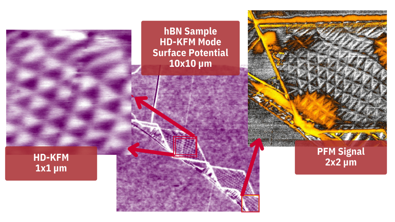
Figure 5 – 10mm size HD-KFM III and PFM measurement of a folded hBN device. Topography shows that surface is atomically flat, while surface potential shows regions with characteristic moiré patterns. This pattern indicates the presence of domains with parallel alignment of the polarization vector. The visible contrast in the SP domains is compatible with AB and BA atomic arrangement (see inset). Alternatively, PFM measurement also shows similar characteristic Moiré pattern.
Advanced AFM Systems from CN Tech
If you're working with Atomic Force Microscopes to perform electrical measurements, the right system can make all the difference. We offer solutions designed with this in mind, including the Nano-Observer Series from CSInstruments, which supports C-AFM, KPFM, PFM and more. These systems combine high-resolution performance with flexible environmental controls. Our team brings deep expertise and practical insight to help you choose the right fit for your application.