Article
10 applications of scanning electron microscopes in modern research
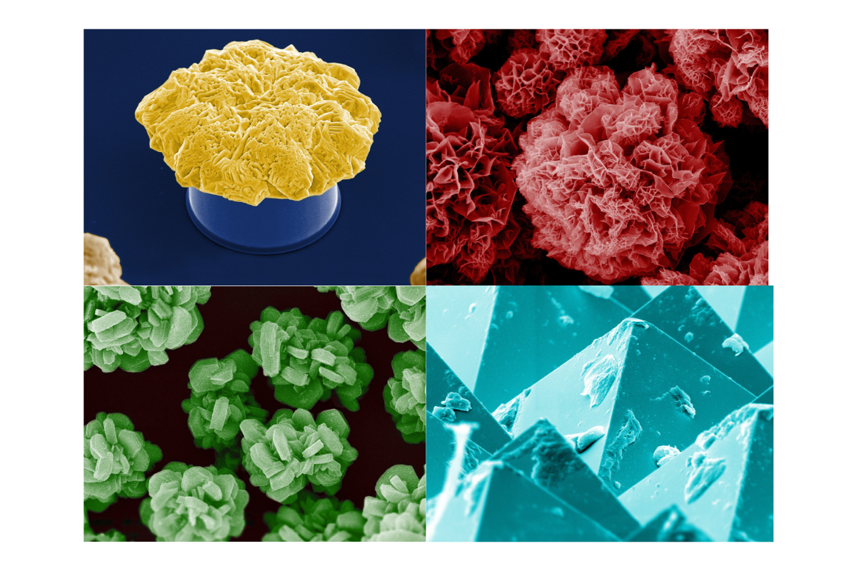
Observing the world at the nanometre scale has redefined what researchers can measure, characterise, and understand. Scanning electron microscopes (SEMs) are central to this transformation. By directing a tightly focused electron beam across a specimen’s surface, SEMS capture high-resolution images that simulate three-dimensionality through their remarkable depth of field, revealing surface features that optical microscopes cannot detect. The signals produced during this process also provide valuable information about a sample’s surface texture, composition, and microstructure.
Beyond simple magnification, SEMs enable researchers to detect microfractures, explore how cells interact with medical implants, and trace the chemical fingerprint of materials drawn from deep within the Earth or recovered from space. Modern research depends on this level of insight, not only to understand the world as it is, but to imagine what it could become.
1. Materials Science and Engineering
Researchers use SEMs to examine microstructures that influence material performance. Grain boundaries, phase separations, and surface coatings often reveal how a material will respond to stress and environmental exposure. High-resolution imaging makes it possible to analyse fracture surfaces, track corrosion onset, and observe wear progression. Moreover, when paired with energy dispersive X-ray spectroscopy, SEMs provide precise elemental data at specific sites. Such information helps engineers design materials that are resilient and efficient.
2. Semiconductor and Microelectronics Research
In semiconductor fabrication, dimensional accuracy and structural integrity are critical. SEMs are used throughout the production pipeline to examine photolithography patterns and detect microscopic defects like particle contamination or layer delamination. High-resolution inspections confirm the integrity of complex architectures and ensure process parameters stay within required limits.
3. Nanotechnology and Nanomaterials
As scientists develop new nanoscale technologies, SEMs provide the visual feedback needed to refine structures and fabrication methods. Researchers use them to examine nanowires, carbon nanotubes, self-assembled surfaces, and modifications to thin films. Within applied settings like nanofabrication labs, this capability becomes crucial for assessing consistency and functionality across structures, revealing morphological variations that may impact performance.
4. Life Sciences and Biomedical Research
Understanding the complex architecture of biological surfaces requires imaging techniques that balance detail with preservation. SEMs meet this challenge by capturing the fine structure of membranes, microbes, and engineered tissues while maintaining sample integrity. Additionally, cryo-SEM and low-vacuum imaging help maintain the moisture content of biological samples, reducing structural changes caused through drying. This is vital in biomedical research, where accurately capturing the interface between tissue and implants supports informed design and clinical decisions.
5. Battery and Energy Storage Research
Charge and discharge cycles introduce microstructural changes that influence the performance of batteries and fuel cells. SEMs allow researchers to observe features such as dendrite formation, cracking, and interface degradation in lithium-ion and solid-state systems. Merged with elemental mapping, this analysis helps identify failure mechanisms and guides improvements in material design for more stable, efficient technologies.
6. Geoscience and Planetary Exploration
Minerals, rocks, and planetary materials often contain microscopic features essential to reconstructing geological history. SEMs reveal textures in sedimentary structures, map mineral zoning, and expose microfossils embedded in ancient formations. Planetary scientists rely on SEM imaging to study the surface composition of meteorites and lunar samples, supporting research into planetary evolution and environmental conditions.
7. Forensic Science and Criminal Investigation
Microscopic evidence including gunshot residue, fibres, and glass fragments can offer vital clues in criminal investigations. With their ability to detect particles below the threshold of optical resolution, SEMs help forensic analysts to study morphology and surface features in remarkable detail. Elemental analysis strengthens the findings, linking materials to their sources and supporting admissibility in court.
8. Additive Manufacturing and 3D Printing
The surface quality and internal structure of 3D printed components can vary depending on the material and printing method. Engineers depend on SEM imaging to study layer interfaces, evaluate powder characteristics in metal printing, and detect issues like voids, cracks, or incomplete fusion. Insights from this analysis aid with the refinement of printing parameters and strengthen mechanical reliability in high-precision environments.
9. Environmental and Agricultural Research
Environmental samples often contain microscopic structures that reveal how ecosystems respond to stress and contamination. The application of SEMs makes it possible to study soil porosity, trace microplastics in water, and examine how pollutants adhere to plant surfaces. Agricultural research uses the same approach to analyse pollen grains, seed coatings, and root systems. This can generate insights that support crop development and sustainable land use.
10. Archaeology and Cultural Heritage Conservation
Preserving historical artefacts requires a clear understanding of their material composition and surface condition. SEMs allow conservators to examine tool marks, corrosion patterns, and pigment residues on ancient objects while also enabling elemental analysis to identify the materials originally used and detect early signs of degradation. Together, these insights inform conservation strategies designed to maintain historical integrity and prevent further deterioration.
Empowering Research with Advanced SEM Solutions
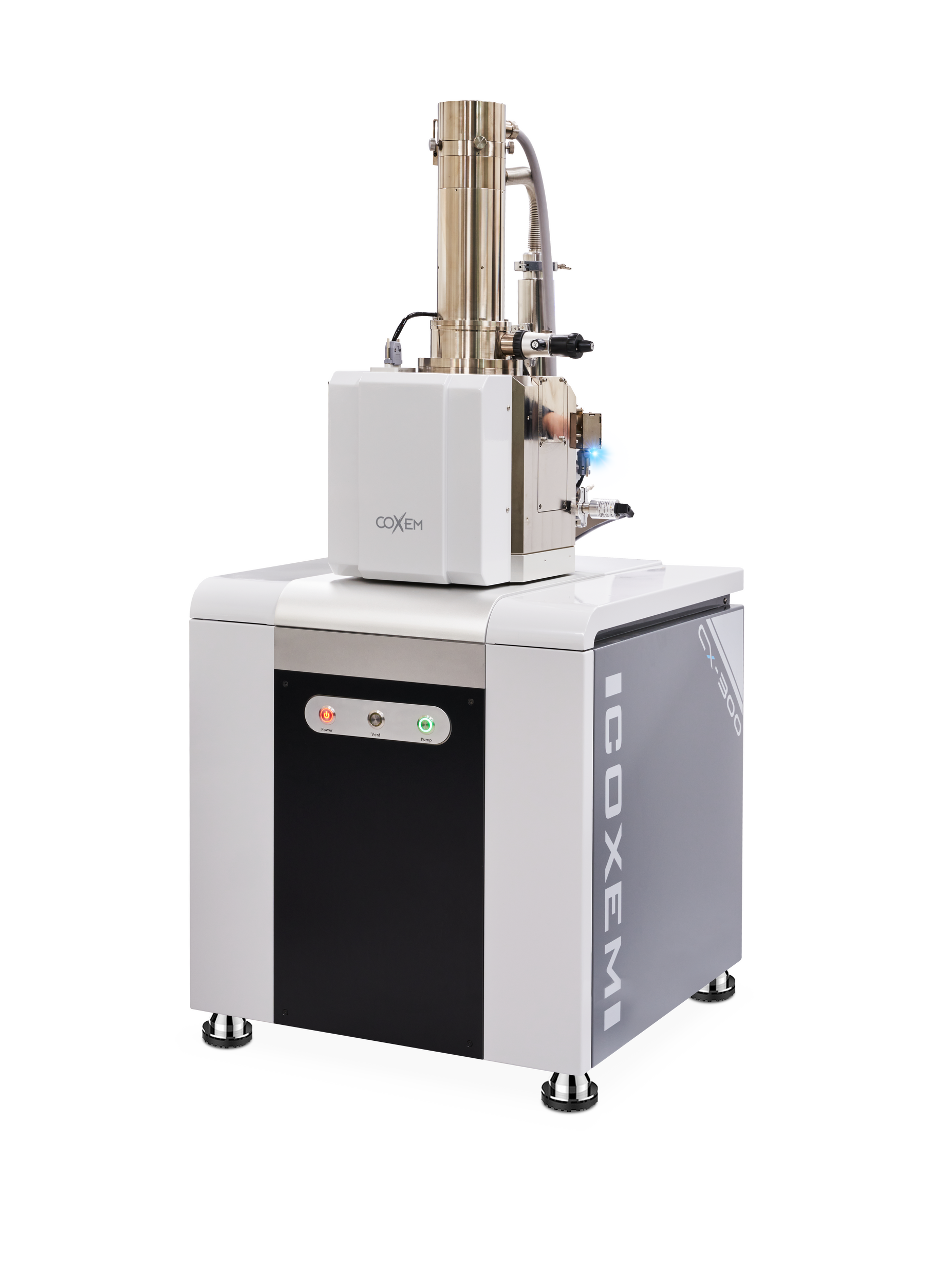
Modern research in materials science, electronics, life sciences, and forensics relies on precise imaging and analysis to answer increasingly complex questions. CN Tech offer SEM systems built to support that work. The CX-300, designed for large-area analysis, offers easy and efficient operation with a maximum magnification of 500,000x. The expanded chamber enhances its versatility, making it ideal for a wide range of research and quality control applications. Combining cutting-edge technology and user-friendly design, the CX-300 sets a new standard for powerful microscopy.
Contact us to learn more about our available SEM's.