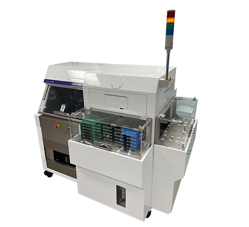
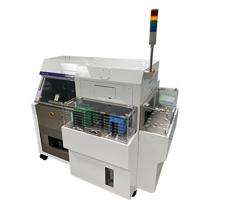
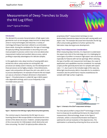
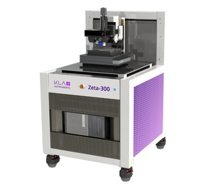
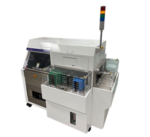
Zeta™-388 True Colour 3D Optical Profiler
The Zeta™-388 is a non-contact, 3D surface topography measurement system. Powered by patented ZDot technology and Multi-Mode optics, the Zeta™-388 is able to measure a variety of samples: transparent and opaque, low to high reflectance, smooth to rough texture, and step heights from nanometre to millimetres.
The Zeta-388 automated optical metrology system integrates six different optical metrology technologies in one configurable and easy-to-use system.
Key Features
- Easy to use non-contact optical profiler with ZDot and Multi-Mode optics to address a wide range of applications
- High-quality microscope sample review or defect inspection
- ZDot: Simultaneously collects a high-resolution 3D scan and a True Colour infinite focus image
- ZI: Zeta phase and vertical scanning interferometry (PSI and VSI) enable wide area measurements with high z resolution
- ZIC: Interference contrast for quantitative 3D data of surfaces with sub-nanometre roughness
- ZFT: Film thickness and reflectance is measured with an integrated broadband reflectometer
- AOI: Automatic optical inspection to quantify defects on the sample
- Production capability: Fully automated measurements with sequencing and pattern recognition
- Wafer handler: Automatically load opaque (e.g. silicon) and transparent (e.g. sapphire) samples, 100mm through 200mm in diameter
Manufacturer
KLA
A global technology leader who make an impact by creating solutions that drive progress and transform industries. Collaboration is the key to their success. KLA provide leading-edge technology and devices using advanced inspection tools, metrology systems, and computational analytics. Their solutions accelerate tomorrow’s electronic devices. They enable evolution and innovation in the data era across key industries including automotive, mobile and data centre.
Product Overview
The Zeta-388 optical profiler is a non-contact, 3D surface topography measurement system. The Zeta-388 builds on the capability of the Zeta-300 with the addition of a cassette-to-cassette handler for fully automated measurements. The system is powered by patented ZDot technology and Multi-Mode optics, enabling measurement of a variety of samples: transparent and opaque, low to high reflectance, smooth to rough texture, and step heights from nanometre to millimeters.
The Zeta-388 automated optical metrology system integrates six different optical metrology technologies in one configurable and easy-to-use system. ZDot measurement mode simultaneously collects a high-resolution 3D scan and a True Colour infinite focus image. Other 3D measurement techniques include white light interferometry, Nomarski interference contrast microscopy, and shearing interferometry.
Film thickness can be measured with ZDot or an integrated broadband reflectometer. The Zeta-388 is also a high-end microscope that can be used for sample review or automated defect inspection.
The Zeta-388 supports both R&D and product environments by providing comprehensive step height, roughness, and film thickness measurements, defect inspection capability, and cassette-to-cassette wafer handling.
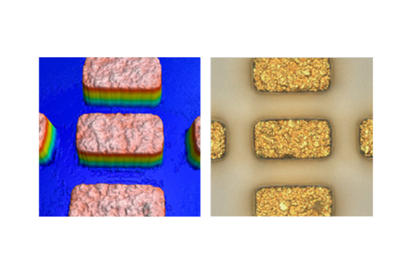
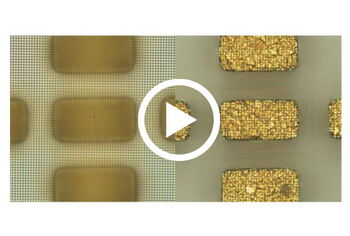
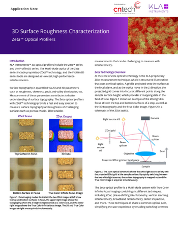
ZDot™ High Resolution 3D Topography & Imaging
With KLA’s patented ZDot™ technology, is possible to collect high resolution 3D topography data simultaneously with True Colour infinite focus imaging. Through a combination of innovative 3D measurement technology, and advanced computer algorithms, high quality surface measurements and imagery is collected with efficiency and accuracy. Combined with the Zeta-388’s automated wafer handling, the Zeta-388 provides high-throughput sample inspection capabilities with incredible clarity.
Shown left: ZDot™ High Resolution 3D Topography Data
Shown Right: ZDot™ Infinite Focus True Colour Imaging

Industries
- Wireless Device Manufacturing for SAW, BAW, and FBAR devices
- LED: light emitting diodes and PSS (patterned sapphire substrates)
- Semiconductor and compound semiconductor
- Semiconductor WLCSP (wafer-level chip scale packaging)
- Semiconductor FOWLP (fan-out wafer-level packaging)
- PCB (printed circuit board) and flexible PCB
- MEMS: Micro-electro-mechanical systems
- Medical devices and microfluidic devices
Applications
Step height
The Zeta-388 is capable of measuring 3D, non-contact step heights from nanometres to millimetres. ZDot and Multi-Mode optics provide a range of methods to measure the step height. ZDot is the primary measurement technique and can quickly measure steps from tens of nanometres to millimetres. ZXI interferometry can be used to measure steps from nanometres to millimetres over a large area. ZSI shearing interferometry can be used to measure steps less than 80nm.

Film thickness
The Zeta-388 is capable of measuring film thickness of transparent film(s) using ZDot or ZFT measurement techniques. ZDot is used to measure transparent films greater than 10µm, such as photoresist or microfluidic device layers that are coated on higher refractive index substrates. ZFT uses an integrated broadband reflectometer to measure films from 30nm to 100µm. This can be done for a single or multiple-layer film stack, with the user entering the properties of the film or using a model to fit the spectrum.
Texture: Roughness and Waviness
The Zeta-388 measures 3D texture, quantifying the sample’s roughness and waviness. ZDot enables measurement of roughness ranging from tens of nanometres to very rough surfaces. ZSI and interferometry enable measurement of smooth surfaces, from angstroms to microns. Software filters separate the measurements into roughness and waviness components and calculate parameters, such as root mean square (RMS) roughness. Nomarski interference contrast microscopy enables visualising very fine surface detail by revealing small changes in the slope.

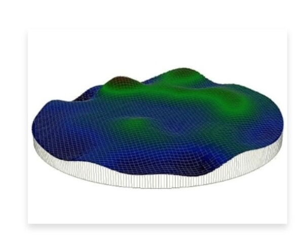
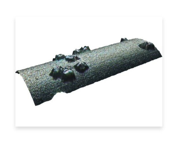
Form: Bow and Stress
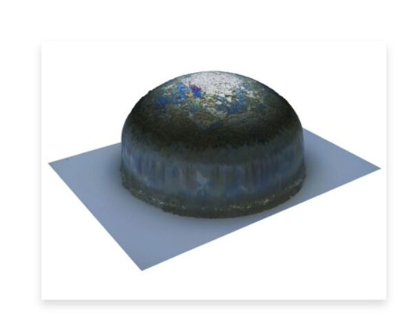
The Zeta-388 can measure the 2D and 3D shape or bow of a surface. This includes measurement of wafer bow that can result from mismatch between layers during the production of semiconductor or compound semiconductor devices. The Zeta-388 can also quantify the 3D height and radius of curvature of structures, such as a lens.
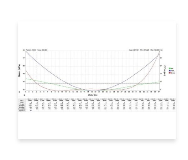
Stress: Thin Film Stress
The Zeta-388 is capable of measuring stress induced during the manufacture of devices with multiple layers, such as semiconductor or compound semiconductor devices. The bow of the surface is accurately measured using a stress chuck to support the sample in a neutral position. The change in shape from a process, such as film deposition, is then used to calculate the stress, applying the principles of Stoney’s equation. The Zeta-388 measures 2D stress by finding the height of the sample surface at user-defined intervals across the full sample diameter and then combining the data into a profile of the sample shape.
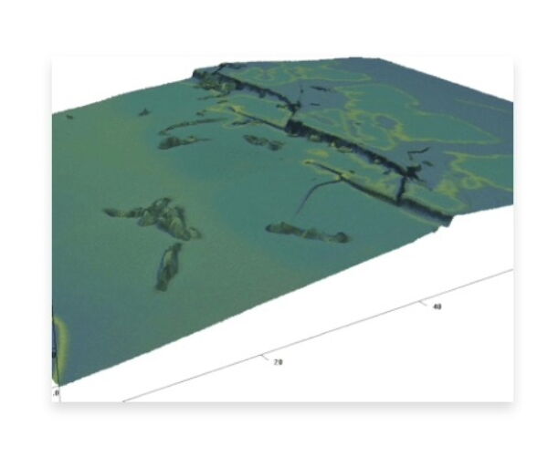
Automated Defect inspection
The Zeta-388 is capable of Automated Optical Inspection (AOI) to rapidly inspect the sample, differentiate different defect types, and map defect density across the sample. When combined with the 3D metrology capability, the Zeta-388 can provide additional information about the defect that cannot be obtained with 2D inspection systems, enabling quicker identification of the defect source.

Defect review
Zeta-388 defect review uses an inspection tool KLARF file to drive the stage to the defect locations. The user can inspect the defect with the high-quality microscope or measure the topography of the defect, such as the height, thickness, or texture. This provides additional detail about the defect that cannot be obtained from a 2D defect inspection system. The Zeta-388 can also mark defects with a scribe, making it easier to find the defect on tools, such as SEM review tools, that have a limited field of view.
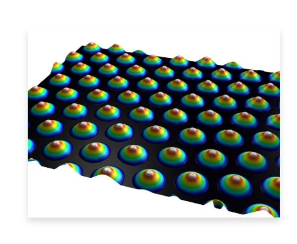
LED Pattern Sapphire Substrates (PSS)
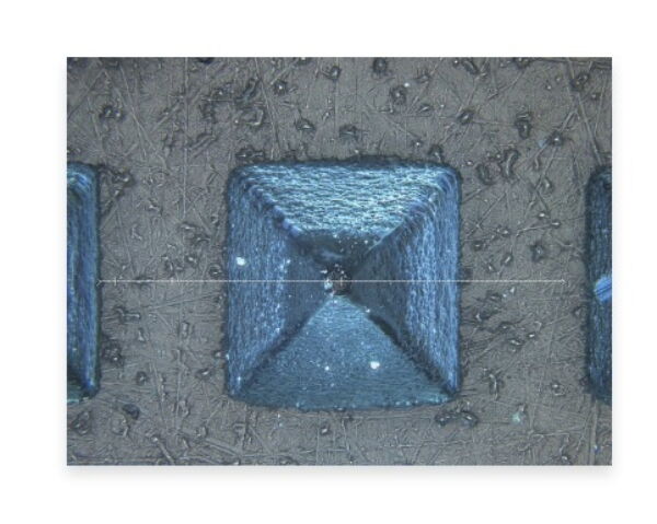
The Zeta-388 optical profiler supports metrology and inspection of patterned sapphire substrates. The system combines ZDot, through-sample lighting and custom algorithms to quickly quantify the height, width, and pitch of PSS bumps. The Zeta-388 can also be used to measure the photoresist before and after patterning, enabling sample rework before sapphire etch. Automated defect inspection of PSS substrates enables rapid identification of critical defects, such as missing PSS bumps, bump bridging, tear-out and contamination. The Zeta-388 includes an automated wafer handling system to reduce operator intervention and contamination from manually handling samples.
Semiconductor and Compound Semiconductor Packaging
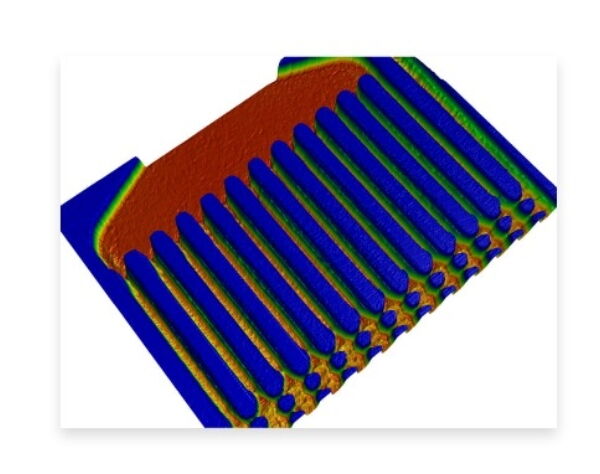
The Zeta-388 supports Wafer-Level Chip Scale Packaging (WLCSP) and Fan-Out Wafer Level Packaging (FOWLP) metrology requirements. A key enabling technology is the capability to measure the height of the plated copper with the dry photoresist film intact. This is accomplished by measuring through the transparent photoresist to the seed layer to measure the height of the copper pillar, thickness of the photoresist, and relative height difference of copper and photoresist. Additional applications include measurement of redistribution lines (RDL), under bump metallization (UBM) height and texture, photoresist opening critical dimension (CD), photoresist thickness, and polyimide thickness. Coplanarity of the metal contacts can also be measured to determine if the bump height meets final device packaging connectivity requirements.
Laser Ablation
The Zeta-388 can measure topography changes induced by laser surface processing for semiconductors, LED, microfluidic devices, PCBs, and more. Lasers have been adopted for precision micro-scale machining and surface conditioning in industries, such as semiconductors, LED, and biomedical devices. For the semiconductor industry, measurement of the height and width of a wafer ID mark is critical to ensuring it can be read successfully throughout numerous processing steps.
Microfluidics
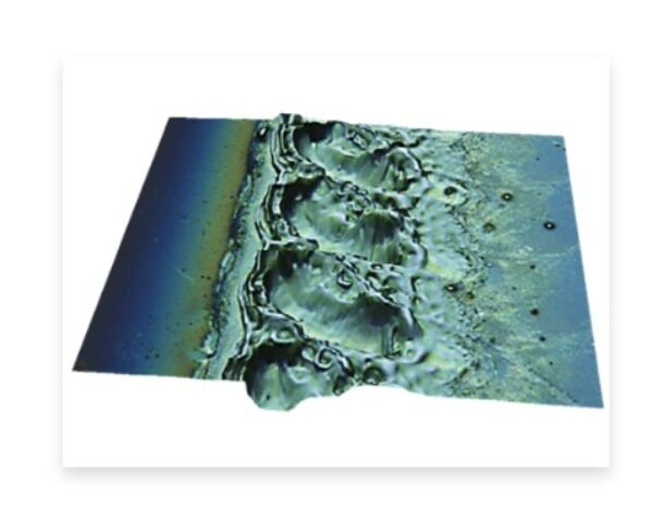
The Zeta-388 has the capability to measure microfluidic devices fabricated in materials, such as silicon, glass, and polymers. The system quantifies the height, width, edge profile, and texture of channels, wells, and control structures. The Zeta-388 can also measure the final device after it is sealed with a transparent top cover plate – compensating for the change in refractive index and quantifying changes from the stress of applying the cover plate.
Biotechnology
The Zeta-388 is well-suited for biotechnology applications, offering non-contact measurement of a variety of sample surfaces having features from nanometres to millimetres. The Zeta-388 can measure high aspect ratio steps, such as the depth of deep wells for biotech devices. Micro-needle array structures for drug delivery can be measured taking advantage of the high numerical aperture objective lens and the ability to resolve a very low reflectance sample.
Videos
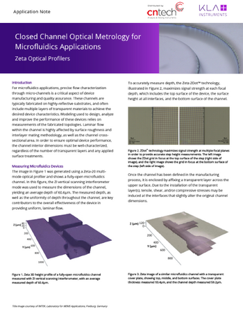
ZDot™
The ZDot™ technology also simplifies operation and setup, by projecting a focusing onto the samples top and bottom surfaces. When the top or bottom surface is correctly focused, the ZDot™ grid will appear in the highest contract, making it fast and intuitive to correctly set up samples. The Zeta-388 is easy to operate, even for less experienced users.
Shown left: The ZDot™ grid visible when the bottom surface is in focus
Shown Right: The ZDot™ grid visible when the top surface is in focus
Downloads
Zeta-388 Optical Profiler Brochure
Zeta-388 Optical Profiler Product Specifications
Objective Lens Selection
Measurement of Deep Trenches to Study the RIE Lag Effect
3D Surface Roughness Characterisation
Closed Channel Optical Metrology for Microfluidics Applications
ZDot™ Technology
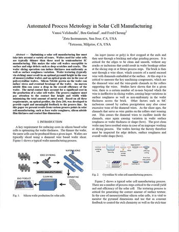
Automated Process Metrology in Solar Cell Manufacturing
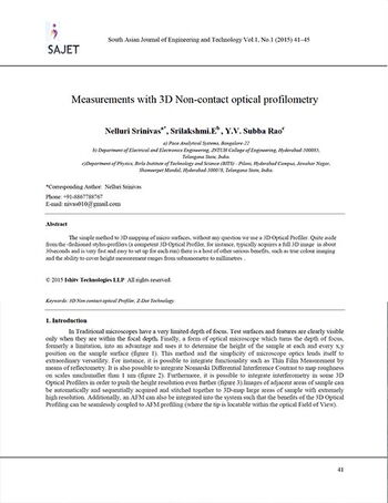
Measurements with 3D Non-contact Optical Profilometry
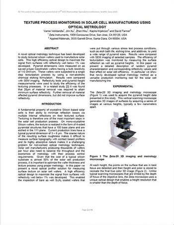
Texture Process Monitoring in Solar Cell Manufacturing Using Optical Metrology
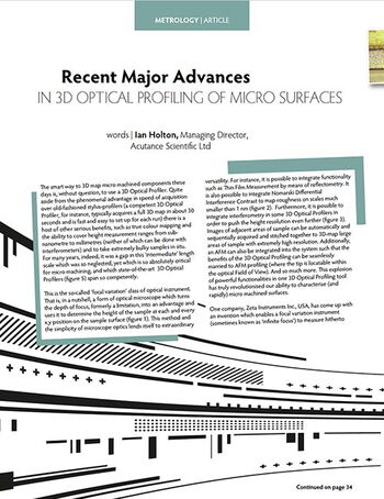
Recent Major advances IN 3D Optical Profiling of Micro Surfaces
Measuring Sealed Micro Fluidic Devices — Yes, It Can Be Done!
How Do You Optimise Your Laser Settings for Precise Micro Manufacturing?
Options
ZFT: Zeta Film Thickness
The Zeta-388 offers an integrated broadband spectrometer for transparent, thin film thickness measurements from 30nm to 100µm. It is capable of measuring single layer or multi-layer stack film thickness with the user selecting the refractive index values from the library of materials. The film thickness can be mapped across the sample to determine the sample uniformity. ZFT works on some of the least reflective surfaces, such as samples with reflectance of less than 0.1%. Many film thickness tools have difficulty obtaining a signal from these type of surfaces, since they depend on specular reflected light to calculate phase change or other parameters. The broadband white light and normal incidence illumination allow the tool to be used for a variety of optically transparent films with low reflectance.

ZI: Zeta Interferometry
The Zeta-388 supports phase scanning interferometry (PSI) and vertical scanning interferometry (VSI) when combined with the piezo stage and an interferometric objective lens. PSI enables fast measurements of step heights from angstroms to hundreds of nanometres. VSI, also known as white light interferometry (WLI), enables measurement of step heights from hundreds of nanometres to hundreds of microns. Both are performed at better than nanometre-level resolution, independent of the objective numerical aperture.

ZIC: Zeta Interference Contrast
The Zeta-388 utilizes Nomarski differential interference contrast microscopy to provide enhanced imaging of fine surface detail. Nomarski microscopy uses polarization and a prism to change the phase to enhance changes in slope on the sample surface. This enables visualization of defects on super-smooth surfaces, such as a monolayer of a contaminant. The ZIC scanning mode can convert these images into quantitative measurements of sub-nanometer level roughness by correlating the change in slope with roughness measured by another technique.

Objective Lenses
A broad range of objective lenses are available including 1.25x – 150x normal objectives, long working distance objectives, ultra-long working distance objectives, refractive index corrected objectives, through transmissive objectives, liquid immersion objectives, and vertical scanning interferometry objectives.

Couplers
The Zeta-388 can be configured with four different optical couplers to change the optics magnification. The system can be configured with the 1x coupler to keep the native magnification, or configured with 0.35x, 0.5x, or 0.63x couplers to increase the magnification.

Objective Lens Turret
The Zeta-388 can be configured with a 5 or 6 position manual turret and an objective lens sensor for automatic objective identification. The system can also be configured with a 6 position motorized turret for fully automated operation.

Sample Lighting
The Zeta-388 uses dual high-brightness white LEDs as standard lighting. Backlighting through the sample chuck is also available to enhance the light for challenging transparent samples, such as patterned sapphire substrates (PSS). The Zeta-388 also supports darkfield

Stages
The Zeta-388 can be configured with a variety of stages to enhance system performance. A piezo Z-axis stage can be added to improve z resolution for measurement of nanometer-level step heights with the ZDot™ or ZXI measurement modes. The XY stage is motorized and can be configured with standard chuck, bowed wafer chuck, or backside illumination chuck.
Sample Chucks
The Zeta-388 has a range of chucks available to support application requirements for samples from 50 to 200mm, including chucks to support bowed wafers. Backlight chucks are available for transparent substrates to support transmitted illumination, required for patterned sapphire substrates. If we do not have the chuck you need, get in touch with your requirements.
Isolation Tables
The Zeta-388 has passive isolation built into the base of the system. For applications requiring better isolation, an active isolation table is available. The Zeta-388 has a standard acoustic enclosure to isolate the system from environmental noise, and to protect the user from sample handler motion.
Step Height and Film Thickness Standards
The Zeta-388 uses thin and thick film NIST traceable step height standards offered by VLSI Standards. The standards feature an etched quartz step with a chrome coating. A step height range of 8nm to 250µm is available. An available certified multi-step standard has nominal step heights of 8, 25, 50, and 100µm. The standard has various pitch patterns for XY calibration. A certified film thickness standard is available for ZFT that includes a reference silicon surface and a nominal 270nm silicon dioxide film thickness. Reference roughness and mirror samples are also available.

Automated Sequencing Software
Automated sequencing software utilizes the motorized XY stage to allow the user to program measurement locations on the sample. The system will automatically measure each site and save the results in user-defined folders. An output report with sample statistics is generated to summarize the results. Advanced sequencing software includes pattern recognition to automatically align the sample. This enables fully automated measurements, reducing the impact of operator error. Auto calibration can also be enabled when using embedded standards on the stage.

Stitching Software
Automated image stitching software utilizes the motorized XY stage to combine adjacent scans to generate a stitched data set that is larger than a single field of view. The system automatically measures every site, aligns the images, and combines them into one data set. The results can be analyzed like any other results file.

Apex Analysis Software
Apex analysis software enhances the tool’s standard data analysis capability with an extended suite of leveling, filtering, step height, roughness, and surface topography analysis techniques. Apex supports ISO roughness calculation methods plus local standards, such as ASME. Apex also serves as a report writing platform with the capability to add text, annotations, and pass/fail criteria. Apex is offered in eight languages.

Offline Analysis Software
The Zeta-388 offline software has the same data analysis and recipe creation capability that exists on the tool. This enables the user to create recipes and analyze data without using valuable tool time.

Related Products
Profilm3D® Optical Profiler | White Light Interferometry
Profilm3D® Optical Profiler | White Light Interferometry
Service Support
Comprehensive repairs and servicing
Annual Support Programs
Your metrology instrumentation is a major investment that is critical to your business operation and success. In today’s competitive climate, it is more important than ever to extend the functionality and peak performance of your metrology equipment years beyond the expiration of your factory warranty. CN Tech’s Support Programs will help ensure that your investment is protected, and that you and your instrument’s are always operating at peak performance.
With over 20 years’ experience servicing and repairing you can be assured that your system is in safe hands. The independent services we offer include system relocation, maintenance visits, parts and consumables, and break down interventions.
CN Tech’s Support Programs are an economical way to guarantee optimal working condition:
- Annual Preventive Maintenance
- Priority Technical Assistance
- Preferred Parts Availability
- On-Site User Training
- Remote Diagnostics
- No surprise repair expense and much more!
Support Contact Example
An example of our service and support contracts are shown below:

Metrology & Instrumentation Annual Support Programs 2024/25
CN Tech's Support Programs will help ensure that your investment is protected, and that you and your instrument’s are always operating at peak performance.