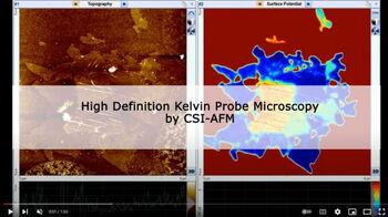
HD-KFM I
HD-KFM™ I is an advanced Kelvin Probe Force Microscopy (KFM) technology designed for the Nano-Observer AFM. This innovative module delivers enhanced sensitivity and resolution in single-pass mode, providing detailed surface potential measurements at the nanoscale.
Key Features
- Single-pass operation for faster acquisition and reduced tip wear
- Enhanced sensitivity and resolution compared to standard double-pass methods
- Bimodal dual-frequency design for optimal performance
- High frequency KFM resonance for improved accuracy
- One-click automated measurement system
Manufacturer
CSI
CSInstruments is a French scientific equipment manufacturer specialised in the conception of Atomic Force Microscope and options designed for existing AFM (Nano-Observer AFM, Resiscope™, High Voltage Amplifier, Magnetic modules). The product range proposed by CSInstruments is designed and manufactured to help the scientific community to achieve nanometre performances that meet the research needs and requirements for actual and future nanoscience applications.
CSInstruments was founded by a team of experts working in AFM field for more than 20 years, starting as pioneer with some historical manufacturers. CSInstruments activity is also based on a qualified and dynamic team, experienced in the fields of mechanics, electronics and data processing. This expertise ensures innovation and performance in the production of AFM and achieves an excellent price/performance ratio!
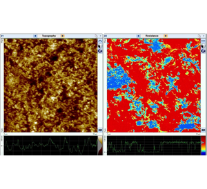
Single-Pass Operation
Single-pass operation in HD-KFM represents a significant advancement over traditional Kelvin Probe Force Microscopy techniques:
Elimination of Lift Scans:
-
Traditional KFM requires two passes: one for topography and another lifted pass for potential measurement.
-
HD-KFM combines both measurements in a single pass, saving time and reducing potential errors.
Proximity to Surface:
-
The tip operates at a typical minimum distance of 0.1-0.5 nm from the sample surface.
-
This close proximity allows for much stronger interaction with the sample's electrostatic field.
-
Compared to standard KFM (10-100 nm lift height), HD-KFM probes an electrostatic field 100-10,000 times stronger.
Enhanced Resolution and Sensitivity:
-
Closer proximity leads to significant improvements in lateral resolution.
-
Sensitivity is greatly enhanced, allowing for detection of subtle variations in surface potential.
-
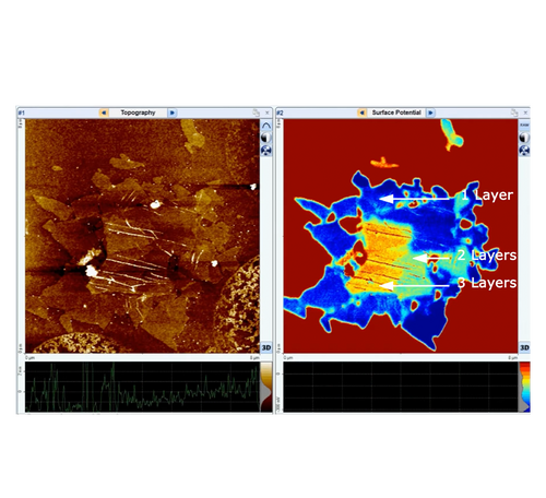
Enables clear differentiation between features like single and multiple layers of 2D materials.
Bimodal Dual Frequency Excitation
Topography Frequency:
-
The first flexural mode of the cantilever is excited mechanically.
-
This frequency is used to measure and control the sample topography.
-
Allows for precise tracking of surface features without interference
Surface Potential Frequency:
-
The second flexural mode of the cantilever is excited electrically.
-
This separate frequency is dedicated to measuring surface potential.
-
Enables simultaneous, independent measurement of topography and surface
Signal Amplification:
-
The use of the second eigenmode for electrical excitation inherently amplifies the signal.
-
This amplification occurs even with very small applied AC voltages.
-
Results in improved signal-to-noise ratio and higher sensitivity to small potential differences.
Enhanced Signal Amplification:
-
The VAC bias is fine-tuned to the second eigenmode of the cantilever.
-
This tuning amplifies the signal by the Q factor of the second mode.
-
The Q factor amplification can be significant, often 100 times or more, greatly enhancing sensitivity.
Improved Stability:
-
The second eigenmode has a stiffer effective spring constant compared to the fundamental mode.
-
This increased stiffness provides more stable oscillation during surface scanning.
-
Stability translates to more reliable and consistent measurements, especially on challenging samples.
Automated Frequency Optimisation:
-
The Vac bias is fine-tuned to the Second eigenmode automatically by the software without user intervention.
-
Patented algorithm selects the best frequency position around the resonance peak.
-
Achieves better resolution and sensitivity through optimised frequency selection.
Specifications
| Technical Parameters | |
| Potential Resolution | < 5mV |
| Spatial Resolution | Down to 10nm |
| Scan Speed | Up to 2 lines/s in single-pass mode |
| Operating Frequencies | First mode: 50-500 kHz, Second mode: 200-1500 kHz |
| Compatible Tips | Metal-coated and highly doped silicon probes |
| System Requirements | |
| Compatible with Nano-Observer AFM systems | |
| Digital controller with high-speed data processing | |
| Automated frequency detection and tracking | |
| Built-in calibration protocols |

Industries
- Materials Science
- Life Sciences
- Semiconductors and Electronics
- Academics
- Others (includes solar cells, geoscience, forensic science, and food technology)
Applications
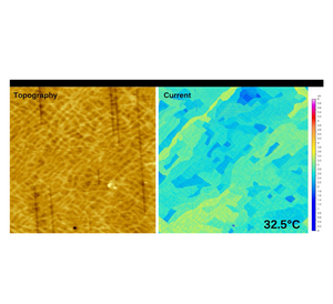
Materials Science
Surface potential mapping, work function measurements, defect detection, thin film analysis
Semiconductors
Doping profiling, device characterisation, failure analysis, nanoscale electronics
2D Materials
Layer identification, electronic property mapping, substrate interaction studies, defect analysis
Polymers
Charge distribution mapping, blend differentiation, aging studies, nanoscale polymer electronics
Life Sciences
Biomaterial characterisation, cell membrane charge mapping, protein/DNA charge analysis, bioelectronics
Videos
HD-KFM Mode
Related Products
Service Support
Comprehensive repairs and servicing
Annual Support Programs
Your metrology instrumentation is a major investment that is critical to your business operation and success. In today’s competitive climate, it is more important than ever to extend the functionality and peak performance of your metrology equipment years beyond the expiration of your factory warranty. CN Tech’s Support Programs will help ensure that your investment is protected, and that you and your instrument’s are always operating at peak performance.
With over 20 years’ experience servicing and repairing you can be assured that your system is in safe hands. The independent services we offer include system relocation, maintenance visits, parts and consumables, and break down interventions.
CN Tech’s Support Programs are an economical way to guarantee optimal working condition:
- Annual Preventive Maintenance
- Priority Technical Assistance
- Preferred Parts Availability
- On-Site User Training
- Remote Diagnostics
- No surprise repair expense and much more!
Support Contact Example
An example of our service and support contracts are shown below:
Metrology & Instrumentation Annual Support Programs 2024/25
CN Tech's Support Programs will help ensure that your investment is protected, and that you and your instrument’s are always operating at peak performance.